上一頁下一頁

全宇宙最好吃的【豆漿優格】來了!
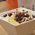
早安!【紅豆蘋果優格】

優格水果早餐...

酸甜美味無法擋的【橘皮果醬竘蒻沙拉】
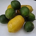
香水檸檬

進攻冰箱之水果早餐。。

364

447

口袋麵包

清冰箱的【彩蔬披薩】

特別烹飪課之【北海道美食】

大家對異國料理的反應很熱烈

異國美食之【焗烤南瓜肉醬】

早餐的白色小船:【洋蔥番茄醬麵】

打破牛排非煎、燒烤不可的【清蒸黑胡椒牛小排】

葡萄牙家常美食:【番茄飯】

2012年最後一個早餐:【和風醬沙拉】

熱情的西班牙【紅椒燉雞肉】

午餐【烤栗子】&【焗烤蒜味櫛瓜番茄】
大人也愛的寶寶副食物:【蘋果馬鈴薯泥】

最佳正餐&下午茶點心:【焗烤馬鈴薯】

迷人的午餐:【焗烤蔬菜】

感動滿滿的高纖早餐:【香檬青芒果洋蔥涼拌沙拉】+【蒸地瓜】

一上桌就後悔的午餐

週末早餐:【番茄檸檬貝殼麵】

最棒的午餐:久違的好友配【泰式雞絲香檬冷麵】

第二頓早餐:【沙拉燒餅】

懶得吃中飯的【焗烤蕃薯】
上一頁下一頁
分享:


郵政劃撥
戶名:國立臺灣大學
帳號:17653341
請填妥捐贈單後,並於劃撥單上的通訊欄註明捐贈相關資訊。 請務必正確填寫捐款用途:
● 捐款用途請點選:其他指定用途
● 說明欄請填寫:開放式課程專用款
● 代碼請填寫:FD101005
如有任何疑問,請打臺大捐款專線:02-3366-9799
臺大捐款網站:http://giving.ntu.edu.tw/donate/index.html
臺大開放式課程感謝您的支持!!
郵政劃撥
戶名:國立臺灣大學
帳號:17653341
請填妥捐贈單後,並於劃撥單上的通訊欄註明捐贈相關資訊。 請務必正確填寫捐款用途:
● 捐款用途請點選:其他指定用途
● 說明欄請填寫:開放式課程專用款
● 代碼請填寫:FD101005
如有任何疑問,請打臺大捐款專線:02-3366-9799
臺大捐款網站:http://giving.ntu.edu.tw/donate/index.html
臺大開放式課程感謝您的支持!!
常見的半導體材料有矽、鍺、砷化鎵等
/
晶片測試
晶片處理高度有序化的本質增加了對不同處理步驟之間度量方法的需求。晶片測試度量裝置被用於檢驗晶片仍然完好且沒有被前面的處理步驟損壞。如果If the number of dies—the 積體電路s that will eventually become chips—當一塊晶片測量失敗次數超過一個預先設定的閾值時,晶片將被廢棄而非繼續後續的處理製程。
/
晶片測試
晶片處理高度有序化的本質增加了對不同處理步驟之間度量方法的需求。晶片測試度量裝置被用於檢驗晶片仍然完好且沒有被前面的處理步驟損壞。如果If the number of dies—the 積體電路s that will eventually become chips—當一塊晶片測量失敗次數超過一個預先設定的閾值時,晶片將被廢棄而非繼續後續的處理製程。
/
步驟列表
晶片處理
濕洗
平版照相術
光刻Litho
離子移植IMP
蝕刻(干法蝕刻、濕法蝕刻、電漿蝕刻)
熱處理
快速熱退火Annel
熔爐退火
熱氧化
化學氣相沉積 (CVD)
物理氣相沉積 (PVD)
分子束磊晶 (MBE)
電化學沉積 (ECD),見電鍍
化學機械平坦化 (CMP)
IC Assembly and Testing 封裝測試
Wafer Testing 晶片測試
Visual Inspection外觀檢測
Wafer Probing電性測試
FrontEnd 封裝前段
Wafer BackGrinding 晶背研磨
Wafer Mount晶圓附膜
Wafer Sawing晶圓切割
Die attachment上片覆晶
Wire bonding焊線
BackEnd 封裝後段
Molding模壓
Post Mold Cure後固化
De-Junk 去節
Plating 電鍍
Marking 列印
Trimform 成形
Lead Scan 檢腳
Final Test 終測
Electrical Test電性測試
Visual Inspection光學測試
Baking 烘烤
/
有害材料標誌
許多有毒材料在製造過程中被使用。這些包括:
有毒元素摻雜物比如砷、硼、銻和磷
有毒化合物比如砷化三氫、磷化氫和矽烷
易反應液體、例如過氧化氫、發煙硝酸、硫酸以及氫氟酸
工人直接暴露在這些有毒物質下是致命的。通常IC製造業高度自動化能幫助降低暴露於這一類物品的風險。
/
Device yield
Device yield or die yield is the number of working chips or dies on a wafer, given in percentage since the number of chips on a wafer (Die per wafer, DPW) can vary depending on the chips' size and the wafer's diameter. Yield degradation is a reduction in yield, which historically was mainly caused by dust particles, however since the 1990s, yield degradation is mainly caused by process variation, the process itself and by the tools used in chip manufacturing, although dust still remains a problem in many older fabs. Dust particles have an increasing effect on yield as feature sizes are shrunk with newer processes. Automation and the use of mini environments inside of production equipment, FOUPs and SMIFs have enabled a reduction in defects caused by dust particles. Device yield must be kept high to reduce the selling price of the working chips since working chips have to pay for those chips that failed, and to reduce the cost of wafer processing. Yield can also be affected by the design and operation of the fab.
Tight control over contaminants and the production process are necessary to increase yield. Contaminants may be chemical contaminants or be dust particles. "Killer defects" are those caused by dust particles that cause complete failure of the device (such as a transistor). There are also harmless defects. A particle needs to be 1/5 the size of a feature to cause a killer defect. So if a feature is 100 nm across, a particle only needs to be 20 nm across to cause a killer defect. Electrostatic electricity can also affect yield adversely. Chemical contaminants or impurities include heavy metals such as Iron, Copper, Nickel, Zinc, Chromium, Gold, Mercury and Silver, alkali metals such as Sodium, Potassium and Lithium, and elements such as Aluminum, Magnesium, Calcium, Chlorine, Sulfur, Carbon, and Fluorine. It is important for those elements to not remain in contact with the silicon, as they could reduce yield. Chemical mixtures may be used to remove those elements from the silicon; different mixtures are effective against different elements.
Several models are used to estimate yield. Those are Murphy's model, Poisson's model, the binomial model, Moore's model and Seeds' model. There is no universal model; a model has to be chosen based on actual yield distribution (the location of defective chips) For example, Murphy's model assumes that yield loss occurs more at the edges of the wafer (non-working chips are concentrated on the edges of the wafer), Poisson's model assumes that defective dies are spread relatively evenly across the wafer, and Seeds's model assumes that defective dies are clustered together.[25]
Smaller dies cost less to produce (since more fit on a wafer, and wafers are processed and priced as a whole), and can help achieve higher yields since smaller dies have a lower chance of having a defect. However, smaller dies require smaller features to achieve the same functions of larger dies or surpass them, and smaller features require reduced process variation and increased purity (reduced contamination) to maintain high yields. Metrology tools are used to inspect the wafers during the production process and predict yield, so wafers predicted to have too many defects may be scrapped to save on processing costs.[26]
游凱復~你已經變性成女的了~好可憐。